Electrochemical STM
Device Specifications
Molecular Imaging / Agilent Setup
- STM 1 um scanner
- AFM 9 um control mode scanner
- EC-STM setup
- Environmental cell for controlled atmospheric imaging
- Ultra-Low Tunneling at 0.5 pA capacity
Technique SOPs
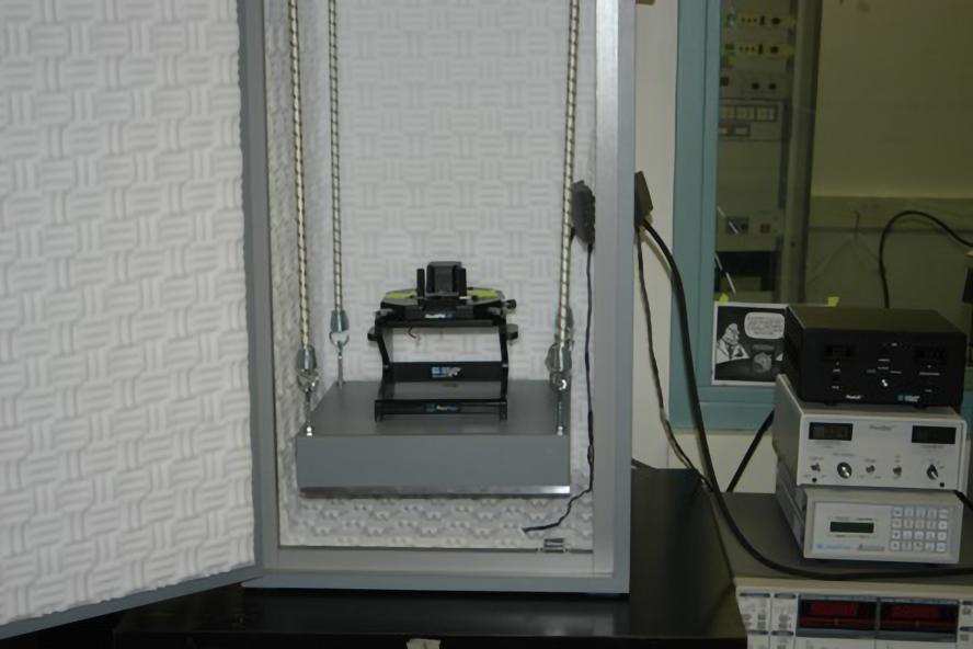
Capabilities
While experiments performed on our UHV/LT STM provide great insight into chemical systems, the operating conditions are not practical for “real world” applications. The advantages of our EC-STM instrument is that it works in an ambient environment (i.e. room temp. and 1 atm.), which makes our results more applicable to industrial processing conditions. We are unable to achieve atomic resolution (except for HOPG) using ambient STMs due to the ease with which metal surfaces become contaminated in air (hydrocarbons and water). This problem can be overcome through the use of in situ STM and EC-STM, both of which involve imaging the surface through a protective liquid layer. EC-STM allows for atomic resolution because in an electrochemical cell the voltage can be swept up and down causing any contaminants on the surface to desorb, hence cleaning the surface. In this way we can replicate the level of surface cleanliness that is routinely obtained in the UHV/LT STM. Once the surface is clean it is possible to add molecules to the electrolyte solution and then study the surface arrangement. Using EC-STM, it is also possible to cycle the potential to measure at what voltages certain molecules adsorb and desorb from the surface.
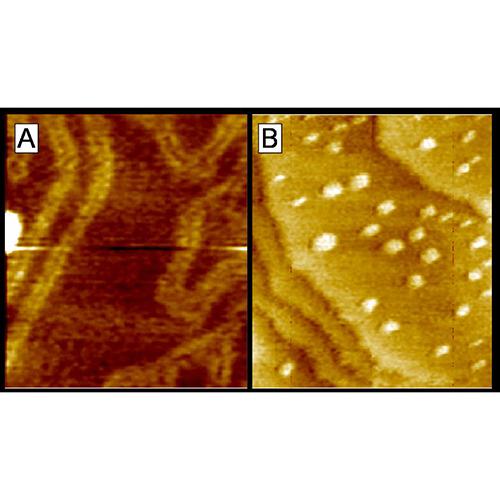
Figure 1A. Au(111) surface in 0.1 M HClO4 and 10 mM benzene imaged at 8.00 nA with a tip bias of 0.1 V, a sample bias of -0.2 V, and a scan size of 50 x 50 nm2. Figure 1B. Same Au(111) surface after >20 minutes at 7.00 nA with a tip bias of 0.0 V, a sample bias of 0.1 V, and a scan size of 150 x 150 nm2. The herringbone reconstruction is lifted by the positive sample bias and as a result Au islands form on the surface.
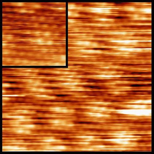
Figure 2A. I monolayer on Au(111) in air imaged at 0.2 nA with a tip bias of -0.05 V and a scan size of 10 x 10 nm2. The moiré pattern arising from a mismatch between the I overlayer and underlying Au atoms is shown in this image. The inset is a 5 x 5 nm2 image showing the atomic resolution of the I monolayer on the Au(111) surface.

Figure 2A. Atomic resolution on Au(111) in 0.1 M HClO4 and 10 mM benzene imaged at 9.0 nA with a tip bias of 0.0 V, a sample bias of -0.3 V, and a scan size of 10 x 10 nm2. The depressions are probably impurities adsorbed on the surface.