How the Scanning Tunneling Microscope Works
The scanning tunneling microscope takes advantage of the tunneling phenomena observed from quantum mechanics to probe any conductive surface with atomic resolutions. Here is how it works:
Classically, when an electron (or for that matter any object) is confronted by a potential barrier that it cannot overcome, such as an electric field, it is stopped and deflected by that barrier. In quantum mechanics, however, we find that the wavefunction (which is the probability amplitude) of the electron can extend into the barrier:
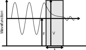
Figure 1. the incident electron does not have sufficient energy to overcome the potential barrier it encounters, nevertheless its wave function extends into and past the barrier. [1]
The implication of this result is that electrons can pass through or "tunnel" through potential barriers by virtue of their probability densities (which are the square of their probability amplitudes). The relaxation of the classical assumption that the probability must be zero in the higher potential region leads to this phenomena, which has been experimentally verified in numerous experiments.
Furthermore, the solutions to the schrodinger equations in these scenarios show that the wave function (and hence probability amplitude) have an exponential decay dependence on distance through the potential barrier. As such, the probability density of the particle is smaller in the region beyond the barrier than the region prior to the barrier. To sum, The probability density of a tunneling particle is exponentially dependent on the width of the barrier it is tunneling through.
As the barrier width decreases the probability density on the opposite side of it, and therefore the current through it, increases exponentially. If this barrier is the gap between the STM tip and a conductive surface, then the distance between the surface and the tip will exponentially relate to the current passing between the two:
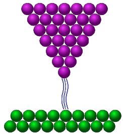
Figure 2. electrons can tunnel between the STM tip (purple) and the surface (green)
Because of this exponential dependence, the device is sensitive to the slight changes in height experienced as the tip moves accross the surface, up and down over atoms and molecules. Tying the tunneling current to the motion of the tip via a z-piezo the motion of the tip (as the tunneling current is held constant) can be measured, telling the experimenter the change in the topographic features of the surface. In this manner the STM is able to obtain atomic resolution images of a conductive surface.
Since we are dealing with the tunneling of electrons, it is easily understood that the STM is also measuring the electron density changes of the surface, an important realization in the understanding of STM images.
- Ingram P, Wilson G and Devonshire R, Appl. Surf. Sci ., 146 , (1999), 363